If you’re a production engineer, you know what matters: repeatable results, rugged equipment, and tools that scale with your line—without surprises.
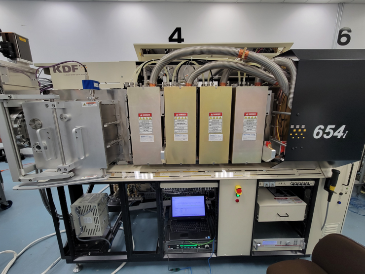
KDF Technologies, part of the Kurt J. Lesker Company, delivers linear in-line sputtering systems that are the gold standard in reliability and performance. Whether you’re coating medical devices, razor blades, or solar display substrates, our systems are built to run—day in, day out—with minimal downtime and maximum consistency.
Why KDF?
✅ Repeatability You Can Rely On
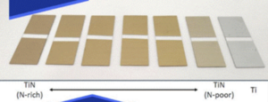
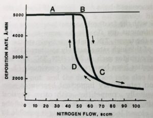
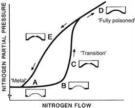
Advanced process control, PEM, and stable reactive gas delivery ensure consistent coatings across batches and substrates.
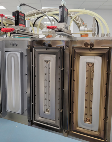
✅ Rugged, Production-Grade Design
Our systems are engineered for real-world manufacturing—built to last, easy to maintain, and ready for high-volume throughput.
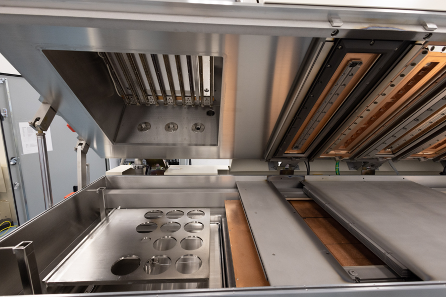
✅ Inline Architecture That Scales
Dual-pallet load-locks, high vacuum pumping, and optional pallet stackers support high-mix, high-volume production with minimal operator intervention.
✅ MRC Legacy, Fully Supported
We are the only provider that fully supports and services legacy MRC sputtering systems—offering upgrades, parts, and process continuity.
✅ Backed by Kurt J. Lesker Company
You benefit from the global support, vacuum expertise, and long-term reliability of one of the most respected names in thin film technology.
Contact Us:
👉 Contact Us
👉 Check out our Systems