• Home
  • Company
    • About KDF
    • Buying from KDF
    • Events
    • Product literature
    • KDF Clientele
    • Worldwide Locations
    • Careers
  • Products
    • PVD and Sputtering
    • Sputtering Products Overview
      • KDF Sputtering Technology
      • Sputtering Products Overview
      • 600i Series Sputtering System
      • 744i Sputtering System
      • 844i Sputtering System
      • 900i Series Sputtering System
      • 974i Series Sputtering System
      • Opus Robotic C2C Loading System
      • Pre-Owned Products
      • Ci Cluster Tool
    • Thin Film Services & Support
      • Original Batch OEM
      • Repair Services
      • Training
      • Thin Film Services
      • Thin-Film Technology
    • Original OEM Parts
      • KDF Upgrade Kits
      • KDF Spare Parts
      • Sputtering Cathodes
      • Sputtering Targets
      • Backing Plates
      • Retrofit Kits
      • PLC Retrofit Kit
    • Process Materials
      • Sputtering Targets
      • Backing Plates
      • Bonding
  • Industries
    • Hermetic Sealing Biocompatible
    • Integrated Passive Devices, Components and Thin Film Circuits
    • Laser Diodes, Photonics and Quantum Technology
    • Medical Device
    • Sensors and Monitoring
    • Wear Coatings
  • News
  • Contact
  • Skip to primary navigation
  • Skip to main content
(201) 784-5005
(201) 784-5005 | sales@kdf.com
REQUEST A QUOTE
KDF electronics inline sputtering equipment
  • Home
  • Company
    • About KDF
    • Buying from KDF
    • Events
    • Product Literature
    • KDF Clientele
    • Worldwide Locations
    • Careers
  • Products
    • custom product dropdown
      PVD and Sputtering
      KDF In-Line Solutions
      KDF Sputtering Technology
      Sputtering Products Overview
      600i Series Sputtering System
      744i Sputtering System
      844i Sputtering System
      900i Series Sputtering System
      974i Series Sputtering System
      Opus Robotic C2C Loading System
      Pre-Owned Products
      Ci Cluster Tool
      Thin Film Services & Support
      Original Batch OEM
      Repair Services
      Training
      Thin Film Services
      Thin-Film Technology
      Original OEM Parts
      KDF Upgrade Kits
      KDF Spare Parts
      Sputtering Cathodes
      Sputtering Targets
      Backing Plates
      PLC-Retrofit
      Retrofit Kits
      Process Materials
      Sputtering Targets
      Backing Plates
      Bonding
  • Industries
    • Hermetic Sealing – Biocompatible
    • Integrated Passive Devices (IPDs), Components and Circuits
    • Laser Diodes, Photonics and Quantum Technology
    • Medical Devices
    • Sensors and Monitoring
    • Wear Coatings
  • News
  • Contact
  • Show Search
Hide Search

Vishal Agrawal

Explanation of Various Sputtering Modes

Vishal Agrawal · July 23, 2021 ·

Written by Ammar Derraa

04/30/2021

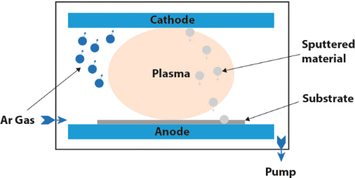
Thin film sputtering, including metal, dielectric, and reactive sputtering can be achieved in one of the following modes: DC sputtering, RF sputtering, Pulsed DC sputtering, and HIPIMS sputtering.

Early mode of sputtering was DC (Direct Current), and represented the simplest and most practical method of metal film deposition. As the demand for thin films application has been growing, sputtering technology has been constantly refined and improved to meet the industry challenges. Today’s sputtering involves many configurations such as, DC magnetron, RF (radio frequency), Pulsed DC, and the newly HIPIMS sputtering. DC magnetron is an enhancement for DC sputtering and does improve the deposition rate. RF sputtering expands the use of sputtering to non-metals. Pulsed DC is another enhancement for DC magnetron mode to optimize reactive processes. The recently-developed HIPIMS sputtering has the advantage of yielding hard coating and enhance step coverage in high-aspect applications.

DC Magnetron Sputtering

The DC sputtering mode in a diode configuration is slow and temperature limited. Magnetically Enhanced Sputtering utilizes a magnetic field that is at right angles to the electric field to increase ionization efficiency in the plasma and confine the electrons near the target. Thus, enhancing the deposition rate without overheat. In fact, Magnetron sputtering offers sputtering rates that are an order of magnitude higher than conventional DC method. This is achieved by a set of magnets mounted on the back of the target.

RF Sputtering

RF sputtering is similar to DC sputtering, but uses an applied RF voltage to eliminate charge buildup on the target. RF sputtering can operate in a diode or magnetron-enhanced configuration. The advantage of reactive sputtering is the ability to sputter dielectric target like quartz.

Pulsed DC Sputtering

Pulsed DC sputtering is used to minimize arcing and target poising in reactive processes. This is achieved by pulsing the applied voltage with a frequency in the range of 1-360kHz. The voltage is reversed for about 1 micron-second to clean any reactive buildup on the target.

Reactive Sputtering

Reactive sputtering refers to the sputtering of a chemically reactive target material in the presence of a reactive gas (usually oxygen or nitrogen) in order to deposit a nitride or an oxide compound film. Since the reactive process can occur in both DC and RF sputtering, either mode can be used for reactive sputtering.  In DC reactive sputtering, chemical reactions do take place on the target surface forming an insulating layer on the target surface. However, in RF sputtering the insulating layer is sputtered away as soon as it forms. Pulsed DC sputtering minimizes this this target poising issue.

HIPIMS Sputtering

HIPIMS (High Power Impulse Magnetron Sputtering) is a new sputtering technique that can produce highly dense, smooth, and hard films with enhanced conformity or step-coverage for high aspect ratio applications. This is the result of a highly dense and ionized plasma that is generated by HIPIMS. In conventional magnetron sputtering, increasing plasma density through power is limited by heat dissipation for any practical gain, and the production of ionized plasma is not a simple task. HIPIMS is based on the use of special power supplies with of a very high voltage to generate short pulses of energy up to a Megawatt peak power. Thus, creating a very highly dense and ionized plasma. KDF has an extensive experience with HIPIMS, and has already developed and optimized many HIPIMS deposition processes along software integration, some of which are currently being used in a manufacturing environment.

What is PVD and Sputtering?

Vishal Agrawal · July 23, 2021 ·

Written by Ammar Derraa

04/30/2021

Introduction to Thin Film Sputtering

Thin film technology is the process of depositing and characterizing functional material layers on a substrate. These layers are the building blocks of modern devices, like computer and cell phone microchips, which require sophisticated know-how and systematic innovation to meet the ever-changing demands of high technology.

Physical Vapor Deposition (PVD) commonly known as sputtering is an established and widely used method in the deposition of thin films and device fabrication.  KDF has many years of experience in PVD or sputtering of thin films. It has the talents and tools to deposit and characterize, with high precision, various films ranging in thickness from a few angstroms to hundreds of microns. This covers most applications requiring thin film coating.

In addition to its state-of-the-art PVD deposition tools, KDF possesses a variety of in-house metrology tools, and has access to an array of test and characterization facilities through its collaboration with research and academic institutions. The R&D team at KDF has a diversified experience in all areas of thin film engineering, devices, process development and characterization, and process integration. KDF research activities are mostly customer oriented and strongly focused on efficient and competitive sputtering technologies to enable production-worthy processes.

Basics of sputtering thin films

Sputtering is one of the most versatile deposition techniques of contemporary thin film technology. It involves the deposition of a material ejected from a source called “target” onto another material called “substrate”.  This is accomplished by a bombardment of the surface of the target with gas ions accelerated by a high voltage.  Particles of atomic dimensions from the target are ejected as a result of momentum transfer between incident ions and the target. The target-ejected particles traverse the vacuum chamber and are subsequently deposited on a substrate as a thin film. Thin film sputtering is carried out in a high vacuum environment with a variety of geometrical shapes and configurations, such as down, up, and side sputtering. KDF offers many sputtering configurations to accommodate different substrate sizes and shapes, as well as custom-made PVD systems. All systems can operate in DC sputtering, RF sputtering, Pulsed DC sputtering, and HIPIMS sputtering.

Simple diagram of a PVD system

[ezcol_1half]

Side sputtering

[/ezcol_1half] [ezcol_1half_end]

Down sputtering

[/ezcol_1half_end]

DC Sputtering Cathode Design

Vishal Agrawal · July 23, 2021 ·

Written by Kurt Flechsig

7/23/2021


DC Magnetron sputtering is a means to achieve higher rates of sputtering over that of diode operation.

KDF offers various cathode designs ranging from sputtering dielectrics, metals and magnetic materials. We have a cathode design that will fit any of your requirements.

Our cathode designs not only take into consideration the sputter rate, but also the utilization and film uniformity as well.

The KDF family of cathodes are of Linear design and span various sizes, starting from 5 x 15 inch, 5 x 17 inch, 5 x 24.5 inch and finally our largest 5 x 30.5 inch cathode.

All of our designs are lab and field proven with thousands of cathodes sold throughout the world. Today’s magnet packs can be comprised of AlNiCo 5, SmCo and NdFe B depending on the application and design of the cathode.

KDF uses all of these types of magnets to create the most productive ionized plasma for a reliable sputter source . When these cathodes are used in KDF inline sputtering systems you can be assured of the best possible outcome of your sputtering job.

KDF Capabilities ‘The Past is Prologue’

Vishal Agrawal · March 2, 2016 ·

KDF was founded in 1986 however it was really born in 1957 with the beginning of Materials Research Corporation, which became a world leader in vacuum processing technology.

As often happens in the cycle of Industry there are births and rebirths with a new enterprise formed from the elements of a past Firm, KDF is one of these. KDF was created during one of the now too common downturns in the Semiconductor industry when the equipment companies discarded anything not perceived as mainstream front-end chip related. Materials Research Corporation, MRC, like others started leaving behind these other applications in pursuit of being the DRAM and CPU ‘Top Gun’ equipment supplier. KDF has, from that beginning, focused on servicing the customer in all aspects from custom integration and system design to individual maintenance planning. KDF has not left behind the semiconductor industry; we have taken the position of not leaving any application that we are capable of supporting and supporting well, behind.

As the large front-end semiconductor companies moved on in their almost single-minded pursuit a vacuum was left behind where customers wanted a ‘technology leader’ or ‘best of breed’ sputtering system but they weren’t necessarily coating silicon wafers. They may have been able to utilize the new cluster tool generation of systems coming out and even if sub-micron high-aspect via filling wasn’t on the wish list the stupendous cost of the systems was simply overwhelming and could not keep them in a competitive position. Here is where KDF has moved in and established a position as a leading provider of small and large area multi cathode inline sputtering systems that are evolved from a world standard MRC design. These systems were the first commercially manufactured semiconductor sputtering system with an installed base that grew to over 3,000 systems worldwide and is still growing today.

KDF today is a system provider to a large and diverse customer base covering a wide range of markets and applications.

Here are some examples; DWDM components, laser diode mirrors, digital micro mirrors, replicated diffraction gratings, Super lattice structures, X-Ray Mirrors, super-bright LEDs, ring laser gyroscopes, high power solid state lasers, large area digital X-Ray detector plates, OLED displays, TFT displays, pace maker components, PZT sensors & actuators, Si , GaAs, Ge and other (all) compound semiconductor devices, micro switches, photo masks, reticules, SAW & BAW devices, hybrids and resistor products, superconductor filters, photovoltaic, MCP night vision optics, MEMS-microsystems-nanotechnology, DNA and other medical sensors, thin film magnetic read write heads, HDI & MCM, multilayer nanocomposites, optical fiber coatings, and more.

KDF is a small company comprised of less than 50 individuals but one that has over 500 person years of experience in-house today and a heritage that goes back to 1957 with thousands of system delivered, hundreds of ‘specials’, dozens of designs and a few truly unique systems.

We at KDF strive to maintain integrity with our customers through our systems and our support as a partner.

Kurt Flechsig
President & CEO

Sign up for the latest updates from us

This field is for validation purposes and should be left unchanged.
logo-kdf-electronics

We offer the most advanced and reliable physical vapor deposition batch in-line sputtering tools at the industry’s lowest cost of ownership. KDF systems can be customized to meet the customer’s needs and cover a wide variety of process requirements for the mainstream silicon, emerging materials and flat panel display markets.

Quicks links

  • About KDF
  • Contact / Quote
  • Our Clients
  • Buying From KDF
  • Worldwide Locations
  • News
  • KDF Events
  • Blog
  • Product Literature
  • Careers

Customer Service & Support

(201) 784-1400

Contact Us

(201) 784-5005
(201) 784-0202
sales@kdf.com
10 Volvo Drive, Rockleigh, NJ 07647
© Copyright KDF Electronic & Vacuum Services Inc. © . All rights reserved.