What Is PVD
and Sputtering?
Physical Vapor Deposition (PVD) sputtering is the foundation of modern thin film manufacturing — used in semiconductor fabrication, medical device production, photonics, sensors, and more. This guide explains how it works and why KDF's inline sputtering systems are trusted by manufacturers worldwide.

What Is Physical Vapor Deposition (PVD)?
Physical Vapor Deposition (PVD) sputtering is the most widely used method for thin film deposition in semiconductor and industrial manufacturing. A solid target material is physically ejected by ion bombardment and deposited as a precise, uniform thin film onto a substrate in a high vacuum environment.
KDF has decades of PVD sputtering experience — with the capability to deposit films ranging from a few angstroms to hundreds of microns across a wide range of materials, substrates, and production environments.
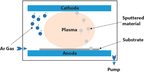
How Does Sputtering Work?
Argon gas is introduced into a vacuum chamber and ionized into a plasma. The positively charged argon ions are accelerated toward the target material, where ion bombardment ejects target atoms that then travel through the chamber and deposit as a thin film on the substrate.
The result is a precisely controlled thin film with excellent adhesion, purity, and uniformity — qualities that make sputtering the preferred deposition method for high-value substrates in semiconductor, medical device, and advanced materials manufacturing.
Sputtering Geometries: Side, Down & Up
KDF inline sputtering systems are available in multiple geometric configurations — each optimized for specific substrate types, film requirements, and production environments.
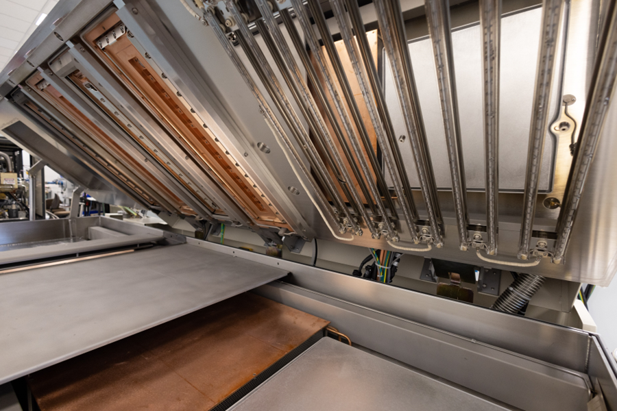
PVD System Overview
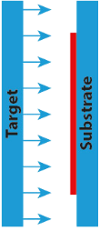
Side Sputtering
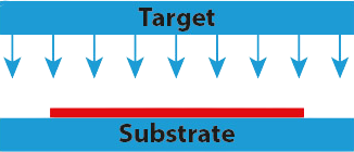
Down Sputtering
Side Sputtering
Targets are mounted on the sides of the chamber, depositing material horizontally onto the substrate. Gravity pulls any particulates away from the substrate surface — making side sputtering the preferred geometry for low-particulate, high-quality PVD thin films in production environments.
Down Sputtering
Targets are mounted above the substrate and deposit material downward. KDF's down sputter systems achieve sub-1% film uniformity with the planetary pallet option — ideal for applications requiring the tightest thickness tolerances across the substrate.
Sputtering Modes — Explained
Modern thin film sputtering encompasses several distinct process modes — each with specific advantages for different materials and applications. All KDF inline sputtering systems support multiple modes on the same platform.
DC Magnetron Sputtering
The workhorse of production thin film deposition. DC magnetron sputtering uses a magnetic field perpendicular to the electric field to increase plasma ionization efficiency and confine electrons near the target — achieving deposition rates an order of magnitude higher than conventional DC sputtering. A set of magnets mounted behind the target generates the confining magnetic field. Best suited for conductive metals and alloys including aluminum, titanium, copper, and molybdenum.
RF Sputtering
RF sputtering applies an alternating radio frequency voltage to the target to prevent charge buildup on the target surface. This enables sputtering of insulating and dielectric materials — such as quartz, alumina, and other non-conductive targets — that DC sputtering cannot process. RF sputtering can operate in both diode and magnetron-enhanced configurations, expanding the range of materials that can be deposited on a single platform.
Pulsed DC Sputtering
Pulsed DC sputtering minimizes arcing and target poisoning during reactive deposition processes. The applied voltage is pulsed at a frequency between 1–360 kHz, with a brief voltage reversal (approximately 1 microsecond) that clears reactive buildup from the target surface before it can form an insulating layer. This results in more stable process conditions, improved film quality, and longer target life when depositing oxides and nitrides.
Reactive Sputtering
Reactive sputtering introduces a reactive gas — typically oxygen (O₂) or nitrogen (N₂) — into the sputtering chamber during deposition. The reactive gas combines with the sputtered target atoms to form compound thin films directly on the substrate. Common reactive sputtering applications include titanium nitride (TiN) for wear-resistant coatings, aluminum nitride (AlN) for piezoelectric devices, and silicon dioxide (SiO₂) for optical and dielectric applications. Reactive sputtering is compatible with both DC and RF modes.
HIPIMS — High Power Impulse Magnetron Sputtering
HIPIMS is an advanced sputtering technique that uses special high-voltage power supplies to deliver short, extremely high-power pulses — up to megawatt peak power — to the sputtering target. This generates a highly dense, highly ionized plasma that conventional magnetron sputtering cannot achieve. The result is thin films with exceptional density, hardness, surface smoothness, and step coverage in high-aspect-ratio features. KDF has extensive HIPIMS process development experience and has deployed optimized HIPIMS processes in active manufacturing environments.
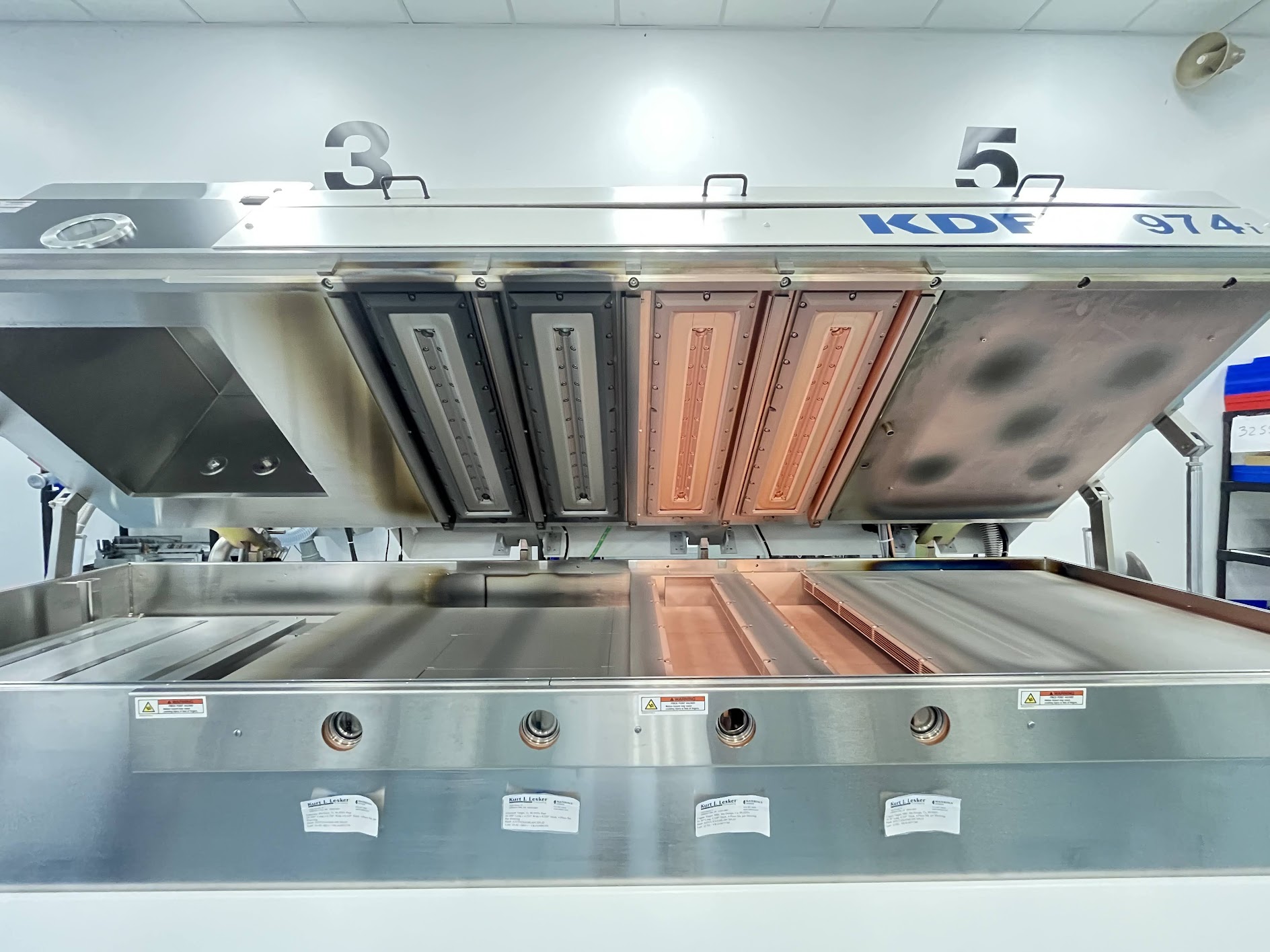
Automated Software Platform
All KDF inline sputtering systems feature a fully automated software platform for tool operation and recipe management — controlling power, pressure, gas flows, timing, and substrate transport with full data logging.
The platform is versatile out of the box and customizable for specific applications, including HIPIMS pulse programming and multi-step reactive processes. KDF's engineers work directly with customers to develop and integrate custom process sequences.
PVD & Sputtering — Frequently Asked Questions
What is Physical Vapor Deposition (PVD)?
Physical Vapor Deposition (PVD) is a vacuum-based coating process in which a solid material is vaporized and deposited as a thin film onto a substrate. Sputtering is the most widely used PVD method in semiconductor and industrial manufacturing. PVD thin films can range in thickness from a few angstroms to hundreds of microns and are used in the production of semiconductors, medical devices, optical components, sensors, and more.
What is the difference between DC magnetron and RF sputtering?
DC magnetron sputtering uses a direct current electric field combined with a magnetic field to confine the plasma near the target, achieving high deposition rates for conductive metals and alloys. RF sputtering uses a radio frequency alternating voltage to prevent charge buildup, enabling deposition of insulating and dielectric materials that DC cannot process. Both modes can be combined with reactive gases for compound film deposition.
What is HIPIMS sputtering and when should I use it?
HIPIMS (High Power Impulse Magnetron Sputtering) uses short, high-power pulses to generate an extremely dense and ionized plasma — producing films with exceptional density, hardness, smoothness, and step coverage. It's the preferred mode for hard coatings, high-aspect-ratio features, and applications requiring superior film mechanical properties. KDF has extensive production-proven HIPIMS process experience.
What is reactive sputtering?
Reactive sputtering introduces a reactive gas (O₂ or N₂) during deposition, causing the sputtered target atoms to form compound films — such as TiN, AlN, or SiO₂ — directly on the substrate. It's compatible with DC, RF, and Pulsed DC modes. Pulsed DC is typically preferred for reactive processes because it minimizes target poisoning and arcing.
What is the difference between side sputtering and down sputtering?
In side sputtering, targets are mounted on chamber walls and deposit horizontally — gravity carries particulates away from the substrate, making it ideal for low-particulate production environments. In down sputtering, targets are above the substrate depositing downward — this geometry excels at achieving very high film uniformity, with KDF's down sputter systems reaching sub-1% uniformity using a planetary pallet option.
What is inline sputtering?
Inline sputtering is a production-oriented PVD architecture where substrates travel through process chambers on pallets in a continuous or batch flow — enabling high-throughput coating of multiple substrates per run with consistent film properties. KDF Technologies specializes exclusively in inline sputtering and operates one of the world's largest installed bases of inline PVD equipment, with 2,000+ systems deployed globally.
Talk to a KDF Sputtering Engineer
Whether you're developing a new thin film process or evaluating inline sputtering systems for production, our team can help you select the right platform and validate your process in our Rockleigh, NJ facility.
Request a Quote View Sputtering Systems