Revolutionizing Thin Film Deposition: How KDF’s ERPP Technology Achieves ±1% Uniformity
Summary:
In the race to meet the ever-tightening demands of microelectronics and optical device manufacturing, precision and repeatability are no longer luxuries—they’re requirements. Enter KDF Technologies’ Enhanced Rotating Planetary Pallet (ERPP), a breakthrough in sputtering system design that delivers metallic film uniformity better than ±1% and repeatability exceeding ±0.5%. By combining advanced planetary motion with linear scanning, the ERPP architecture redefines what’s possible in thin film deposition. Whether you’re engineering multilayer conductive barriers for integrated circuits or optimizing titanium tungsten coatings for acoustic filters, this next-generation platform ensures unmatched consistency, surface quality, and process control. Discover how ERPP is setting a new standard for deposition excellence.
Metallic coatings deposited using the KDF Enhanced Rotating Planetary Pallet (ERPP) exhibit exceptionally high film uniformity and tight process repeatability. This performance is driven by the synergistic effect of the concomitance of the planetary revolution and the system’s standard linear scanning mode. KDF Technologies has developed both reactive and non-reactive sputtering processes for metallic, semi-metallic, semiconductor, and dielectric materials. These processes consistently achieve film uniformity better than ±1% across the pallet, with repeatability exceeding ±0.5% from pallet to pallet. With this capability, we ensure high-performance processing of multilayer conductive barriers and contact materials essential for integrated circuits, in addition to delivering premium titanium tungsten films for adhesion and diffusion applications in both microelectronics and decorative technologies. Furthermore, the flexible programmability of the rotating motion will be examined in the context of its impact on improving deposition uniformity and tailoring surface morphology. With the ongoing evolution of thin-film device applications, deposition tools must meet progressively tighter specifications, delivering superior film uniformity and process repeatability to support next-generation performance.
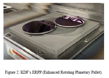
To address these demands, the KDF 900 series sputtering tools employ a combination of linear scanning and sophisticated rotating motion, as illustrated schematically in Figure 1. The novel scanning planetary substrate motion, enabled by the Enhanced Rotating Planetary Pallet (ERPP) ensures that all areas of the substrate are exposed to the sputtered material from various angles. It averages out angular distribution of sputtered atoms while the linear motion compensates for the non-uniform erosion of the target and non-uniform plasma density. Both combined maximize exposure to sputtered flux from all directions and averages out any spatial non-uniformities in the sputtering plume. We demonstrated pallet uniformity and run-to-run repeatability on the order of ±1% across a variety of metallic deposition processes, including tungsten (W) and titanium tungsten (TiW). These system advances now enable the precise and repeatable processing of complex multilayer metallic coatings, supporting critical applications such as optical devices and semiconductor components with exceptional uniformity.
Process with Standard Deposition
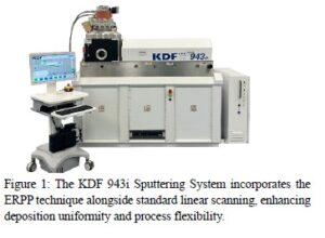
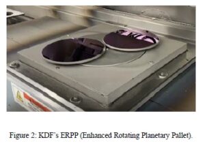
On standard KDF sputtering tools, metallic films such as tungsten (W) and titanium tungsten (TiW) are typically deposited onto a 12” × 12” pallet deposition zone, which scans across a 15” × 5” rectangular magnetron cathode. Deposition is performed via DC magnetron sputtering—either reactively using oxygen or nitrogen with elemental targets, or non-reactively from compound targets. The cathode is specifically engineered to optimize uniformity for metallic films, achieving an average thickness variation of approximately ±2% across four 4” wafers mounted on a planetary rotating pallet. Figure 2 presents a 6” wafer configuration of KDF’s Enhanced Rotating Planetary Pallet (ERPP) system.
Process with System Enhancement
In advanced microelectronic applications, tungsten (W) films are commonly employed as critical layers within frequency-selective components such as surface acoustic wave (SAW) and bulk acoustic wave (BAW) filters. For Solidly Mounted Resonator (SMR) configurations in BAW filters, multilayer silicon-based stacks with exceptional film uniformity and run-to-run thickness repeatability—on the order of ±1%—are required. Since the resonant frequency is inversely proportional to the thickness of the constituent layers, including tungsten, precise thickness control is essential for accurate frequency tuning. KDF 900 series sputtering systems, equipped with three- or four-target configurations, precisely controlled scan speeds, and multistep recipe capabilities, are well-suited for such demanding deposition tasks, offering fine resolution in film thickness across complex multilayer stacks.
To achieve stringent film uniformity targets without incorporating uniformity apertures, a new pallet design was introduced: the Enhanced Rotating Planetary Pallet (ERPP). The ERPP maintains the linear translation characteristic of standard KDF systems.
On top of the pallet sits a rotating platform, referred to as the ‘sun,’ which can rotate continuously over a broad range of speeds. Mounted to this platform are four wafer holders—each accommodating a 4-inch-diameter wafer—referred to as ‘planets.’ Each planet rotates at a fixed gear ratio relative to the sun, generating a full planetary motion of the wafers within the deposition plane. This motion is superimposed onto the standard linear translation of the pallet underneath the target. By integrating both rotational and translational movement, the planetary architecture averages out the spatial variations in deposition rate across the cathode, effectively enhancing uniformity across all wafers. It reduces the edge to center thickness variation. We are anticipating the step coverage on 3D features to be improved as well as we are varying the incident angle of the deposition while rotating. Figure 2 illustrates the schematic configuration of the Enhanced Rotating Planetary Pallet.
Results
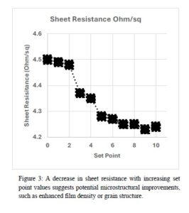
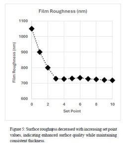
Tungsten (W) and titanium tungsten (TiW) films were deposited non-reactively using elemental W and TiW targets. Figures 3 through 5 summarize the results obtained using the Enhanced Rotating Planetary Pallet (ERPP) technique. Figure 3 illustrates a reduction in sheet resistance with increasing setpoint values under constant linear scanning conditions. Wafer rotation during sputtering was found to significantly enhance thin-film uniformity. This rotational motion helps average out the spatial non-uniformities inherent in the sputtering process, thereby improving thickness uniformity and stabilizing critical film properties such as sheet resistance.
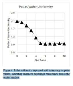
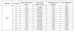
Figure 4 presents the uniformity results for tungsten and titanium tungsten films deposited with the ERPP-enabled KDF 900 system. The planetary scanning motion consistently achieved within-wafer uniformities better than ±1% and pallet-wide uniformities better than ±2%. These results confirm the system’s capacity for high-precision film deposition. Table 1 summarizes the performance of planetary scanning for TiW depositions using standard 15-inch cathode.
In addition, Figure 5 demonstrates significant improvements in surface roughness. While wafer rotation contributes to enhanced thickness uniformity, its influence on surface roughness is multifaceted. Depending on process parameters—such as rotation speed, deposition pressure, and target power—surface roughness may either increase or decrease. Therefore, careful optimization of sputtering conditions is essential to achieve the desired film characteristics for each specific application.
Discussion
We have presented a detailed evaluation of metallic film deposition using a novel planetary scanning substrate carrier. This technique has significantly improved film uniformity and run-to-run repeatability. Specifically, it has enabled us to reduce metallic film uniformities from typical values of ±2% to less than ±1% across the pallet for non-reactive deposition processes.
The planetary deposition technique has potential applications for various other films, and we are currently investigating its advantages for optical films and features with high aspect ratios. Additionally, the ERPP may be integrated with a Plasma Emission Monitoring system and DC Pulsing.

